半導体・パッケージデバイス検査装置 Semiconductor Package Device Inspection
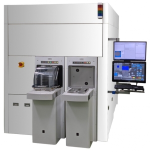
半導体カセットFOUP/FOSB寸法検査装置 (Wafer Cassette Inspection System)
Wafer Cassette FOUP/FOSB Inspection System
- 概要
- ウェハカセットFOUP/FOSB/OCの外径寸法測定を行う装置です(ウェハ挿入済み可)
様々な角度から、トップフランジ、サイドフォークリフトフランジ、ウェハ搭載の段ピッチやレジストレーションピンホールを測定・検査します
It measures the outer diameter of wafer cassettes FOUP/FOSB/OC (cassettes with wafers already inserted can also be measured).
Measures and inspects top flanges, side forklift flanges, wafer mounting step pitch and registration pinholes from various angles.
カタログPDF - 仕様
- ・各種メーカーのFOUP/FOSB/OCに対応
φ300mmの定型サイズ以外やカラーカセットも検査可能
・2500万画素カメラ+専用光学エンジンにより、高画質での外径寸法を可能に!
・超広視野高速処理により、業界最速レベルのスループットを実現
・Can measure FOUP/FOSB/OC from various manufacturers.
Can also inspect non-standard sizes of φ300mm and color cassettes
・25MP camera + dedicated optical engine enables high-quality outer diameter measurements!
・Ultra-wide field of view, high-speed processing realizes the fastest throughput in the industry
SiCウエハー欠陥検査装置 (SiC Wafer Defect Inspection System)
開発中 2026年4月 デモンストレーション開始
SiC Wafer Defect Inspection System
- 概要
- SiC基板およびSiCエピ層に存在するデバイスの特性に致命的な不良を引き起こす欠陥を早期に検出し、プロセスへのフィードバックをかけるレーザーラマン,コンフォーカル微分干渉顕微鏡を搭載した装置です。
コンフォーカルDICによる表面欠陥の検出やPL(フォトルミネッセンス測定)によるEpi欠陥の検出のみならず、サブストレートの欠陥検出も可能です。
また、ラマン分光法を組み合わせることにより、より詳細な欠陥の分析ができます。
---------------------------------------------------------------
[Overview]
This equipment is equipped with a laser Raman and confocal differential interference microscope that detects defects in the SiC substrate and SiC epitaxial layer at an early stage, which can cause fatal defects in the device characteristics, and provides feedback to the process.
This allows us to detect not only surface defects by Confocal DIC and epitaxial defects by PL (photoluminescence measurement), but also defects in the substrate.
In addition, by combining it with Raman spectroscopy, it provides us with more detailed defect analysis results. - 用途
- SiC基板品質として近年問題になっているSiC基板表面下の加工変質層(SSD:Sub-Surface Damage)の存在(表面から10um前後まで変質)。
SSDが残存していると、その上のエピ成長時の積層欠陥形成、基底面転位(BPD : basal plane dislocation)の伝搬の原因となります。
本装置は Raman測定による基板表面深さ方向の残留応力測定が可能。
また、Raman測定によるエピ膜近傍のLocal stress測定、エピ膜表面深さ方向のキャリア濃度 測定も可能です。
---------------------------------------------------------------
[Use]
The presence of a process-affected layer (SSD: Sub-Surface Damage) under the surface of the SiC substrate (affected from the surface to about 10um) has become an issue in recent years in terms of SiC substrate quality. If SSD remains, it can cause stacking faults during epitaxial growth on top of it and the propagation of BPD.
This equipment can measure residual stress in the depth direction of the substrate surface by Raman measurement.
It can also measure local stress near the epitaxial film and carrier concentration in the depth direction of the epitaxial film surface by Raman measurement.
ウエハーレビュー装置 / Wafer Review Equipment
Wafer Review Equipment
- 概要
- ウエハ外観検査装置から提供された情報に基づき、NG画像の詳細な解析・解析データ保存・上位ホストPCと通信
鮮明な画像データをAI機能で、自動判定可能。
[Overview]
Device for detailed analysis of NG images, storage of analysis data, and communication with host PC based on information provided by wafer inspection system. - 用途
- 半導体デバイス・CMOSデバイス製作工程での欠陥管理
[Use]
Defect management in semiconductor device / CMOS device manufacturing process - 仕様
- 対応ワークサイズ : 12インチ/8インチ
---------------------------------------------------------------------------
ワーク状態 : Wafer ダイシング
---------------------------------------------------------------------------
ステージ位置決め精度 : ±1um
---------------------------------------------------------------------------
レビュー精度 : 3σ ≦ ±20um
*欠陥情報座標に対する位置決め精度
---------------------------------------------------------------------------
スループット : 約2000秒(10枚処理)
*欠陥数 : 100/枚
*Reference 画像撮像Mode
*欠陥場所により変化
---------------------------------------------------------------------------
レビュー(移動~AF~撮像)時間 : 最速0.5秒
*欠陥場所により変化
---------------------------------------------------------------------------
[Specification]
Applicable work size: 12 inch / 8 inch
-------------------------------------------------- -------------------------
Work state: Wafer dicing
-------------------------------------------------- -------------------------
Stage positioning accuracy: ± 1um
-------------------------------------------------- -------------------------
Review accuracy: 3σ ≤ ± 20um
* Positioning accuracy for defect information coordinates
---------------------------------------------------------------------------
Throughput: Approximately 2000 seconds (10-sheet processing)
* Number of defects: 100 / piece
* Reference imaging mode
* Depends on defect location
---------------------------------------------------------------------------
Review (moving to AF to imaging) time: fastest 0.5 seconds
* Depends on defect location
---------------------------------------------------------------------------
The System takes defect images and the datum are upladed to the upstream system.
The defect infomation is provided by Wafer Review System and Wafer Inspection System; AVI.
The System also analyzes the defect information from AVI.
Seiwa SAWR Series inspect your application at high speed with high precision.
We can also manufacture AVI.
The defect infomation is provided by Wafer Review System and Wafer Inspection System; AVI.
The System also analyzes the defect information from AVI.
Seiwa SAWR Series inspect your application at high speed with high precision.
We can also manufacture AVI.
表裏パターンずれ検査装置 / Double Side Alignment Inspection
Double Side Alignment Inspection
- 概要
- 両面露光後の表裏パターンのズレ、貼り合せ後のウエハのズレを表裏各々の方面から同時にズレ量を計測
(TOP-BOTTOM計測)
表面レイヤー露光後のアライメントズレも計測(TOP-TOP計測)
カセットtoカセットタイプ、セミオートタイプも用意
薄いワーク、反り易いワークにもオプション対応致します。
[Overview]
Simultaneously measure the amount of misalignment of the front and back patterns after double-sided exposure and the misalignment of the wafer after bonding from both sides (Top-Bottom measurement).
Measurement of alignment deviation after surface layer exposure (TOP-TOP measurement)
Cassette to cassette type and semi-auto type available
Possible to handle thin and easily warped workpieces as option. - 用途
- 半導体デバイス
CMOSデバイス
センサーデバイス製造工程での表裏パターンニング精度管理」
[Use]
Semiconductor device
CMOS device
Front and back patterning accuracy control in
sensor device manufacturing process - 仕様
- Waferサイズ Maxφ12インチ
---------------------------------------------------------------------
測定再現性精度 10X 0.2μm/3σ(Top-Bottom)
20X 0.02μm/3σ(Top-Bottom)
---------------------------------------------------------------------
画面計測箇所 25箇所
---------------------------------------------------------------------
レシピ管理数 2,000個
---------------------------------------------------------------------
スループット Top-Top 100枚/h
*5点計測 Top-Bottom 100枚/h
---------------------------------------------------------------------
[Specification]
Wafer size Max φ12 inch
-------------------------------------------------- -------------------
Measurement repeatability 10X 0.2μm / 3σ (Top-Bottom)
20X 0.02μm / 3σ (Top-Bottom)
---------------------------------------------------------------------
Screen measurement location 25 positions
---------------------------------------------------------------------
Recipe number 2,000
---------------------------------------------------------------------
Throughput Top-Top 100 sheets / hour
* 5 points measurement Top-Bottom 100sheets / hour
---------------------------------------------------------------------
マイクロLED検査&リペア装置 / μ LED Inspection & Repair
μ LED Inspection & Repair
- 概要
- MINI/μ-LEDのマストランスファー後のChip検査、Chip除去、Chip再マウントをする装置
[Overview]
After mass transfer of MINI / μ-LED, this machine perform chip inspection, chip removal and chip remounting. - 用途
- 大型ディスプレイのMINI/μ-LEDのデバイス完成に対して、ディスプレイを修正する装置
[Use]
Equipment to modify the display for the completion of MINI / μ-LED devices
for large displays - 仕様
- 検査工程:LED Chipの検査
Chip 有/無
Chip 位置ずれ
Chip 汚れ
Particle
PL(フォトルミネッセンス)
Chip除去:レーザー照射による、半田の溶融し、除去
Chip再マウント:Micro LED 15×25μ~100μ、Mini LED 100μ~1000μm
[Specification]
Inspection process: LED Chip inspection
Chip Yes / No
Chip misalignment
Chip dirt
Particle
PL (photoluminescence)
Chip removal: Laser irradiation melts and removes solder
Chip remount: Micro LED 15×25μ~100μ, Mini LED 100μ~1000μm
狭ベゼル対応レーザーボンディング装置 / Laser Bonding for Slm Bezel Display
- 概要
- ヒートシンク式溶着の進化版の、レーザーボンディング装置。
周辺にダメージを与えず、均一性の高い圧着が可能。
[Overview]
Laser bonding equipment, an advanced version of heat sink type welding.
Highly uniform crimping is possible without damaging the periphery. - 仕様
- 搭載レーザー;LDレーザー
Laser照射幅;0.3mm×25mm
均一性 ;90%以上
[Specification]
Onboard laser; LD laser
Laser irradiation width; 0.3mm × 25mm
Uniformity; 90% or more
ダイレクトレーザーソルダリング装置 / Direct Laser Soldering
- 概要
- リフロー後の検査で、ノーボールの場合、半田ボールを再搭載し、レーザーでダイレクトにソルダリングを行います。
[Overview]
Inspect and find the position of No (absent) ball after reflow,
remount solder ball and perform soldering directly by laser to the proper position. - 仕様
- 検査 ;On Fry検査
ボール搭載 ;1SEC以下
搭載レーザー;LDレーザー
[Specification]
Inspection ; On Fry inspection
Ball mounted; 1sec or less
Onboard laser; LD laser
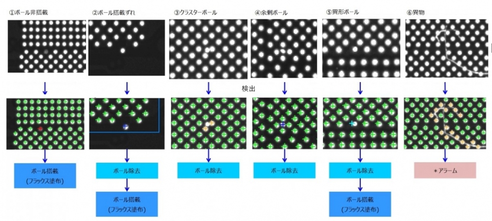
ハンダボールリペア装置 / Micro Solder Ball Repair Equipment
Micro Solder Ball Repair Equipment
- 概要
- 高密度実装用プリント基板・ウエハに実装されたマイクロボールの高速検査とリペアを行います。
ボール非搭載、搭載位置ずれ、ボールクラスター、余剰ボール、異径ボール、異物を検出し、高速でリペアを行います。
[Overview]
High-speed Micro Solder ball inspection and repair for high-density mounting printed circuit boards and wafers.
Detects non-ball mounted, mounting position shift, ball cluster, surplus ball, different diameter ball, Contamination, and performs high-speed repair. - 用途
- パッケージデバイス、FOWLPなどのバンプ形成工程
[Use]
Bump formation process for package devices, FOWLP, etc. - 仕様
- 対応ボールサイズ φ40µm~φ500μm
----------------------------------------------------------------
対応基板サイズ PCB:500mm×500mm
シリコンウエハ:12inch
----------------------------------------------------------------
検査及び欠陥修正項目
[Specification]
Corresponding ball size: φ40μm - φ500μm
----------------------------------------------------------------
Available board size PCB 500mmx500mm
Silicon wafer: 12inch
----------------------------------------------------------------
Inspection and defect correction items